VLSI
VLSI Technology basically stand for Very large scale integration i.e. 1 Million (10lac) of transistors on a 1 mm2 silicon area.
Very-large-scale integration (VLSI) is the process of creating an integrated circuit (IC) by combining thousands of transistors into a single chip. VLSI began in the 1970s when complex semiconductor and communication technologies were being developed. The microprocessor is a VLSI device.
Before the introduction of VLSI technology, most ICs had a limited set of functions they could perform. An electronic circuit might consist of a CPU, ROM, RAM . VLSI lets IC designers add all of these into one chip.
The electronics industry has achieved a phenomenal growth over the last few decades, mainly due to the rapid advances in large scale integration technologies and system design applications. With the advent of very large scale integration (VLSI) designs, the number of applications of integrated circuits (ICs) in high-performance computing, controls, telecommunications, image and video processing, and consumer electronics has been rising at a very fast pace.
The current cutting-edge technologies such as high resolution and low bit-rate video and cellular communications provide the end-users a marvelous amount of applications, processing power and portability. This trend is expected to grow rapidly, with very important implications on VLSI design and systems design.
A fab lab (fabrication laboratory) is a small-scale workshop offering digital fabrication
Cost of Fablab – Typical fablab require 3-4 billion$ (1 billion $ = 5000 Crores Rs.)
Clean room is extremely important in FABlab.
Yield :
University level fabrication – it may be upto 25 % i.e. 5 chips in out of 20 are working
Industry level fabrication – it has to be almost 98 to 99 % ; Very high yields are expected
Semiconductor world Market generates revenue of 300 billion $ wherein they produce Microprocessors, memories, ICs etc.
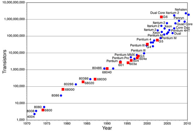
Moore’s Law
“The number of transistors embedded on the chip doubles after every one and a half years.”
The number of transistors is taken on the y-axis and the years in taken on the x- axis.
“The number of transistors embedded on the chip doubles after every one and a half years.”
The number of transistors is taken on the y-axis and the years in taken on the x- axis.
CMOS Scaling parameters
- Functionality : Mobile : camera, video, voice recording, large memory, Accelerometer, GPS
- Size : reducing
- Performance : Speed: up
- Cost : down – that is the driving force: consume less silicon: reduce cost per transistor
(10 million or 1 billion transistor in a chip ; Cost /transistor) - Power : decreasing (does not always happen)
