Clean Rooms
- Particles that might deposit on silicon wafer and cause a defect may originate from many sources including people, machines, chemicals and process gases.
- Unwanted Impurities must be kept below the ppm or ppb range and stray particles must be essentially eliminated. Modern IC factories employ a three tiered approach to control unwanted impurities:
1. Clean Rooms 2. Wafer Cleaning 3. Gettering - Class definition: Class X means that in each cubic foot of air in the factory, there are less than X total particles greater than 0.5 micrometer in size. Typically particles of size 10nm to 10 micron size are present in the semiconductor plants.
- Recirculate air at certain times / hr. Replace air 100 times / hr. for class 500.
- Single dust particle of 20nm may damage the device/ckt.
- Building clean rooms is very expensive. It requires air handling systems and filters, and other huge equipment.
- Maintenance at regular intervals is necessary. They always work at higher pressure; must be always ON, thus large electricity bills
how do we minimize the particles?
- People in the plant wear “bunny suits”. Often face masks and individual air filters are used are worn to prevent exhaling particles into room air.
- Air showers at the entrance blow loose off particles off the people before they enter.
- Constant air filtration is used to remove particles as they are generated. This is done through HEPA filters (High Efficiency Particulate Air ). Its composed of thin porous sheet of ultrathin glass fibres. Small particles stick to these fibers primarily through electrostatic forces.
- Particles may be introduced in wafer cleaning process. Deionized water is used for wafer cleaning. Resistivity in the range of 17 to 18 Megaohms. Ion exchangers or reverse osmosis is used to remove ionic species.
WAfer cleaning
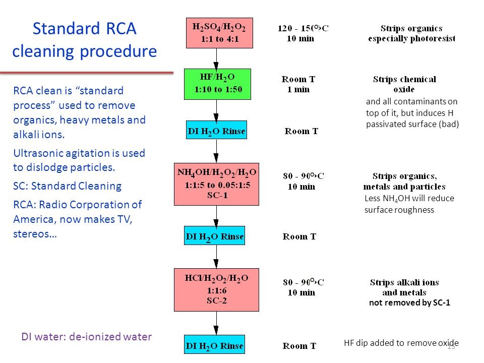
- In order to remove metallic impurities, organic contaminants etc. wafers were subjected standard RCA cleaning procedure.
- All chemicals are MOS grade. Ex. Of company J.T. Baker. Resistivity of DI water 17-18 MOhm-cm.
- Most cleaning procedures begin with photoresist removal since photolithography normally precedes each processing step. For front end processing (no metals on wafer).
- First method uses an H2SO4 and a strong oxidant (usually H2O2) to decompose the resist Into CO2 and H2O.
- The second method uses an oxygen plasma to convert resist to gaseous byproducts (again CO2 and H2O. This reduces pollution problems. Used in removal of photoresist in backend processes.
- Wafer cleaning is usually accomplished today either using immersion of cassettes of wafers into cleaning baths or through chemical sprays.
Front end cleaning
–Front end processes often involve high temperatures (oxidations, anneals, film deposition etc. )
–These steps allow diffusion of contaminants into thin films on the silicon or into the silicon itself.
–Therefore, cleaning process must remove contaminants prior to these steps.
Back end cleaning:
–These processes are normally low temperature, so the wafer cleaning, though imp, is not critical.
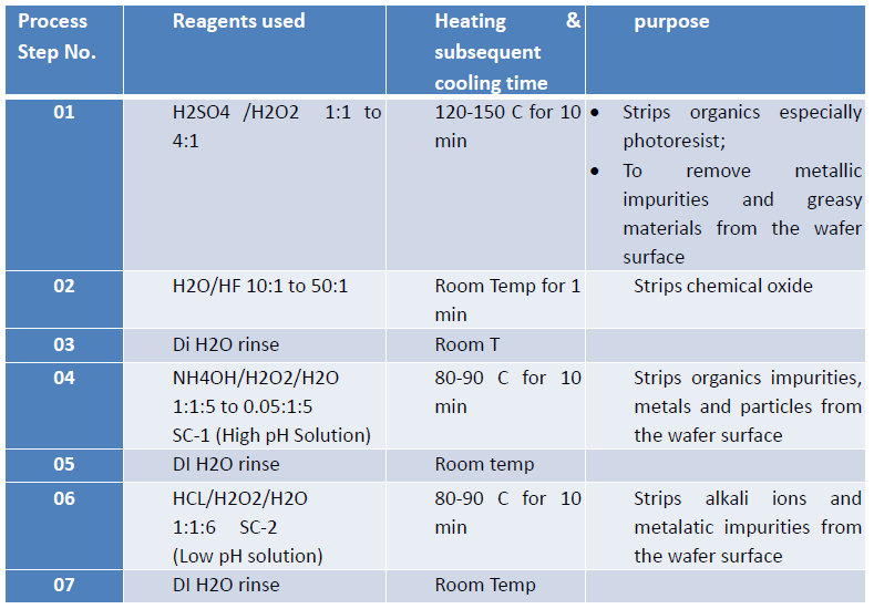
RCA Cleaning Process