DIAC
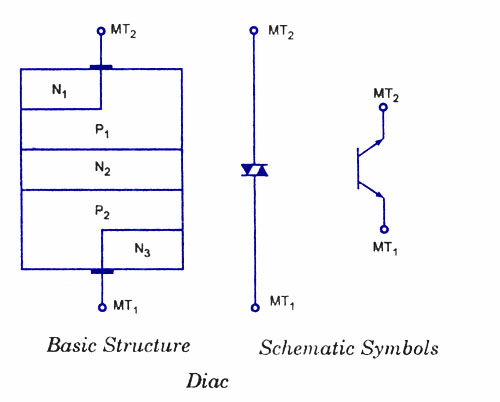
Construction
· Diac is a 2- terminal device.
· Parallel inverse combination of semiconductor of layers that permits triggers in either direction. ( from MT1 to MT2 or MT2 to MT1 )
· The two SCRs formed are N1P1N2P2(MT1 TO MT2)and N3P2N2P1 (MT2 TO MT1)
· Diac is a 2- terminal device.
· Parallel inverse combination of semiconductor of layers that permits triggers in either direction. ( from MT1 to MT2 or MT2 to MT1 )
· The two SCRs formed are N1P1N2P2(MT1 TO MT2)and N3P2N2P1 (MT2 TO MT1)
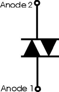
Symbol
Operation
· When MT1 is positive with respect to MT2, conduction takes place through P1N2P2N3 which is a p-n-p-n device.
· When MT2 is positive with respect to MT1, conduction takes place through P2N2P1N1.
· Device can be turned ON either in positive half cycle or –ve half cycle of an AC voltage( or it can be turned on for two breakover points (VB0 and –VB0) )
· For (+ve) half cycle, if applied voltage < VB0, a very small current called leakage current flows through the device.
· It is produced through the drift of e-and holes in the depletion region and is not sufficient to cause conduction.
· Hence, DIAC is in blocking state.
· When in DIAC applied voltage reaches VB0, current increases and voltage decreases
· This region is the conducting state for pnpn device in the forward blocking state.
· The breakover voltage for a diac is always constant.
· Hence, there is no gate terminal.
· For –ve half cycle, we get exactly similar characteristic in 3rd quadrant.
· Forward characteristic is similar to that of a 4- layer pnpn device which is in 1st quadrant.
· Reverse characteristic appear in 3rd quadrant. It is anti-symmetric to characteristic IQ.
· VBO ranges from 20V to 40V.
· Time required to turn ON DIAC is 50 nanoseconds to 500 nanoseconds.
· Time required to turn OFF DIAC is about 100 nanoseconds.
· Power handling capacity – 300W to 1W.
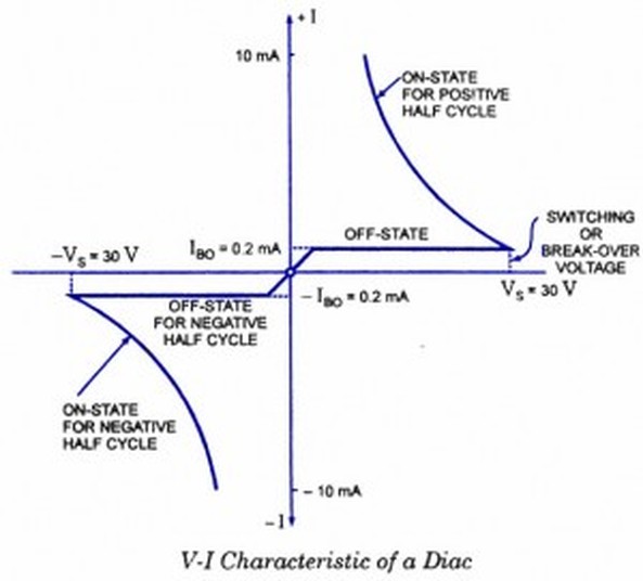
V-I Characteristics
