FIELD EFFECT TRANSISTORS
- FET is a transistor that uses an electric field to control the shape and hence, conductivity of a channel of one type of charge carrier in a semiconductor material.
- FETs are Unipolar transistors.
- It is a voltage operated device.
- It is a 3 – terminal device.
- FETs are Unipolar transistors.
- It is a voltage operated device.
- It is a 3 – terminal device.
3 Terminals of FET
· Source : Carriers enter the channel current.
· Drain : Carriers leave the channel current.
· Gate : Terminal that modulates the channel conductivity.
· Source : Carriers enter the channel current.
· Drain : Carriers leave the channel current.
· Gate : Terminal that modulates the channel conductivity.
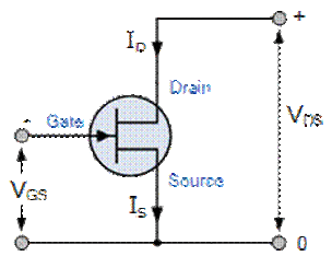
Circuit Diagram
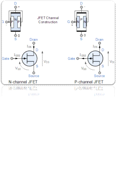
JFET
- Junction Field Effect Transistor
- Has No p-n junctions
- JFETs have a channel which carries current
- Channel is a narrow piece of high resistive semiconductor material
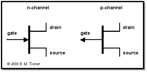
Symbol
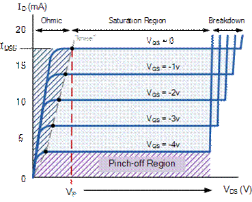
Output Characteristics
|
|
MOSFET
· Metal Oxide Semiconductor Field Effect Transistor · It has a metal oxide gate which is electrically insulated from the main semiconductor · Also known as IGFET |
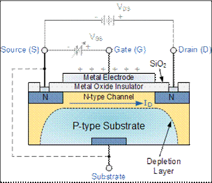
MOSFET Construction
TYPES OF MOSFETs
Depletion mode
Transistor requires Gate-Source voltage to switch the device OFF
Equivalent to normally CLOSEDswitch
Enhancement mode
Transistor requires Gate-Source voltage to switch the device ON
Equivalent to normally OPEN switch
Depletion mode
Transistor requires Gate-Source voltage to switch the device OFF
Equivalent to normally CLOSEDswitch
Enhancement mode
Transistor requires Gate-Source voltage to switch the device ON
Equivalent to normally OPEN switch
MODES OF FETS
The field effect transistor being a three terminal device is capable of three distinct modes of operation.
1) Common Source (CS) Configuration
2) Common Gate (CG) Configuration
3) Common Drain (CD) Configuration
ADVANTAGES OF FET
· High input resistance (of the order of 100 MΩ or more)
· FET typically produces less noise than a BJT.
· Relatively immune to radiation.
· Exhibits no offset voltage at zero drain current .
· Better thermal stability.
· FETs are easier to manufacture than the BJT
DISADVANTAGES OF FET
· Relatively low gain-bandwidth product compared to a BJT.
· Vulnerable to electrostatic damage during handling.
· Dissipate large amounts of power while switching.
· Poor frequency response due to its high input capacitance.
· FETs have a very poor linearity, and generally they are less linear than BJT.
USES OF FET
· Audio frequency amplifiers and in high input impedance pre-amps and stages.
· Switching Internal combustion engine ignition coils.
· CMOS range of digital logic chips.