POWER ELECTRONICS
Power electronics devices are capable of handling very large current and voltage drops. They devices are used in high power applications like converters, buffers, inverters. Typical current ratings are in the range of several 100s of amperes.
Power electronics devices are capable of handling very large current and voltage drops. They devices are used in high power applications like converters, buffers, inverters. Typical current ratings are in the range of several 100s of amperes.
P-N-P-N Diode
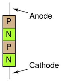
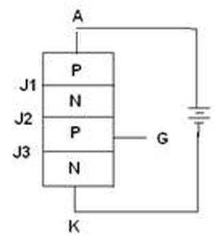
· It is a 4-layer device consisting 4 alternate layers of p-type and n-type materials as shown in figure.
· P and N regions on extreme regions are called anode (A) and cathode (K) respectively.
· If anode is made positive with respect to cathode then junctions J1 and J3 are in forward biased.
· This applied voltage then effectively appears across te junction J2. Junction J2 is reverse biased.
· If the applied voltage (Vak) is increased then a stage comes when semiconductor junction J2 breaks down.
· Breakdown occurs when the reverse voltage exceeds the peak inverse voltage (PIV) of the diode.
· At this breakdown, current (Iak) increases suddenly from a small value to a large value.
· This increase in current is accompanied with an increase in voltage which gives rise to a small negative resistance region.
· The point at which this happens is reffered to as ‘Breakover point’. It is the point when the PNPN device switches from its OFF state to its On state.
· There are 3 regions of operation of a PNPN device –
1. Cut-off region – Current through the device is ideally zero and practically very small. The cut-off region extends till the breakover voltage.
2. Transition region – When Anode-cathode voltage exceeds breakover voltage, device switches rapidly from cut-off region to saturation region. PNPN device will remain in this state for a very small time. It is also known as the negative resistance region.
3. Saturation region – Once the device is breakover, device remains in this state till current remains above the holding current value i.e. the PNPN device saturates.
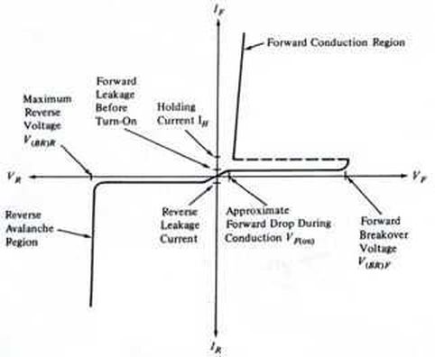
Characteristics
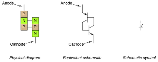
Two transistor analogy of a PNPN device
THYRISTORS
Thyristors are solid state devices which have more than one p-n junction. These junctions can be switched from a non-conducting state to a conducting state using an appropriate anode-cathode voltage and maintaining a proper current through it.
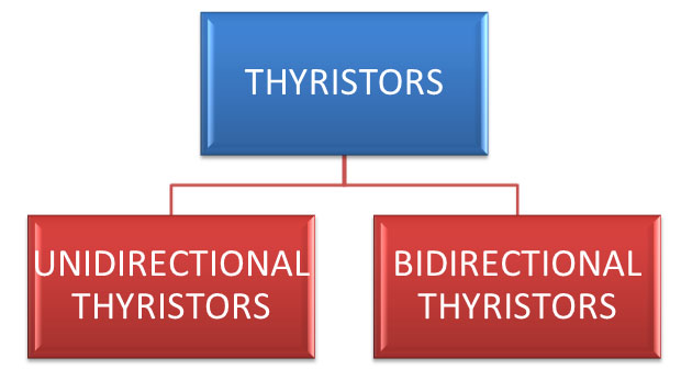
CLASSIFICATION OF THYRISTORS
Thyristors can be divided into two types –
1. Unidirectional thyristors
· SCRs (Silicon controlled rectifiers)
· GTO ( Gate turn OFF thyristors)
· LASCR ( Light activated SCR)
2. Bidirectional thyristors
· DIAC
· TRIAC
Thyristors are solid state devices which have more than one p-n junction. These junctions can be switched from a non-conducting state to a conducting state using an appropriate anode-cathode voltage and maintaining a proper current through it.
CLASSIFICATION OF THYRISTORS
Thyristors can be divided into two types –
1. Unidirectional thyristors
· SCRs (Silicon controlled rectifiers)
· GTO ( Gate turn OFF thyristors)
· LASCR ( Light activated SCR)
2. Bidirectional thyristors
· DIAC
· TRIAC
SILICON CONTROLLED RECTIFIER (SCR)
Construction and working
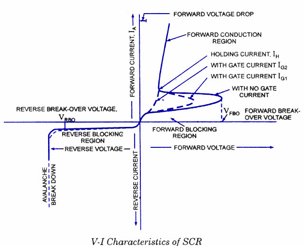
· When anode (A) is made positive with respect to cathode (K), junction J1 & J3 are forward biased.
· Leakage current can flow only through reverse biased junction J2.
· SCR is in OFF state (Forward blocking state) when junctions J1 & J3 are forward biased and J2 is reverse biased.
· If supply voltage is increased further, SCR turns ON at a particular voltage known as the breakover voltage (Vbo).
· When cathode is made positive with respect to anode, J1 & J3 are reverse biased and J2 is forward biased.
· Her, small reverse leakage current flows through the SCR.
· In this mode, SCR can support entire supply voltage across it.
· SCR is in ON state (reverse blocking state).
· When Vak is increased, J2 which is reverse biased will break down due to large voltage gradient across the depletion layer.
· This is the reverse breakdown which can damage the SCR if the SCR does not have a proper dimension, critical doping and good cooling solution.
· At the same time, if a current is injected into the gate, SCR turns ON.
· When SCR is turned on, SCR dos not support any forward voltage drop across it. This is true for an ideal SCR.
· Practically, in ON state, SCR has a forward voltage drop of 1-2 V.
· Device is now said to be in Forward Conduction Mode (saturation).
· Current flows from anode to cathode.
· Once SCR is turned ON, gate current loses control over the device.
· The only way to turn the SCR OFF is by reducing the current below the holding current value. This method of turning OFF SCR is known as SCR commutation. It is done by commutation circuits.
· Latching current – The minimum anode current required to maintain SCR in ON state immediately after the SCR has turned ON and gate signal has been removed is known as latching current.
· Holding current – The minimum anode current required to hold SCR in ON state is known as holding current.
Construction and working
· When anode (A) is made positive with respect to cathode (K), junction J1 & J3 are forward biased.
· Leakage current can flow only through reverse biased junction J2.
· SCR is in OFF state (Forward blocking state) when junctions J1 & J3 are forward biased and J2 is reverse biased.
· If supply voltage is increased further, SCR turns ON at a particular voltage known as the breakover voltage (Vbo).
· When cathode is made positive with respect to anode, J1 & J3 are reverse biased and J2 is forward biased.
· Her, small reverse leakage current flows through the SCR.
· In this mode, SCR can support entire supply voltage across it.
· SCR is in ON state (reverse blocking state).
· When Vak is increased, J2 which is reverse biased will break down due to large voltage gradient across the depletion layer.
· This is the reverse breakdown which can damage the SCR if the SCR does not have a proper dimension, critical doping and good cooling solution.
· At the same time, if a current is injected into the gate, SCR turns ON.
· When SCR is turned on, SCR dos not support any forward voltage drop across it. This is true for an ideal SCR.
· Practically, in ON state, SCR has a forward voltage drop of 1-2 V.
· Device is now said to be in Forward Conduction Mode (saturation).
· Current flows from anode to cathode.
· Once SCR is turned ON, gate current loses control over the device.
· The only way to turn the SCR OFF is by reducing the current below the holding current value. This method of turning OFF SCR is known as SCR commutation. It is done by commutation circuits.
· Latching current – The minimum anode current required to maintain SCR in ON state immediately after the SCR has turned ON and gate signal has been removed is known as latching current.
· Holding current – The minimum anode current required to hold SCR in ON state is known as holding current.
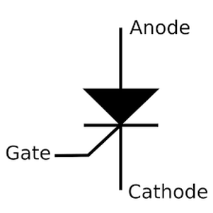
Symbol
Characteristics
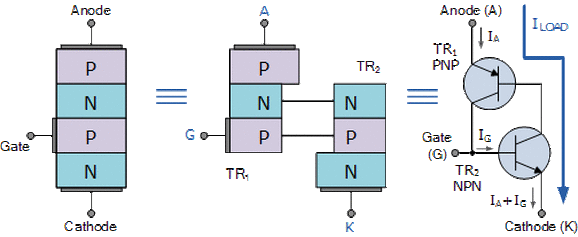
Two transistor analogy of a SCR
