introduction to 8051 Microcontroller
A microcontroller is an economical computer-on-a-chip built for dealing with specific tasks, such as displaying or receiving information through LEDs or remote controlled devices. The most commonly used set of microcontrollers belong to 8051 Family. 8051 Microcontrollers continue to remain a preferred choice for a vast community of hobbyists and professionals. Through 8051, the world became witness to the most revolutionary set of microcontrollers. The Intel MCS-51 (commonly termed 8051) is a Harvard architecture, complex instruction set computing (CISC) instruction set, single chip microcontroller (µC) series developed by Intel in 1980 for use in embedded systems.
Features of 8051 -
Features of 8051 -
- 8051 is a 40 pin IC
- It works on +5V DC voltage and TTL logic
- 8-bit Microcontroller
- It has clock generator on chip (6,8,12,24 MHz)
- It has 128 bytes RAM on chip (expandable upto 64kB)
- It has 4 kB ROM on chip (expandable upto 64kB)
- 1 Full duplex serial port (Modes 01,2,3)
- 4 8-bit I/O ports
- 8051 has 8 Special Function Registers (SFRs)
- 2 Timers and 6 Interrupt sources
Pin Diagram of 8051
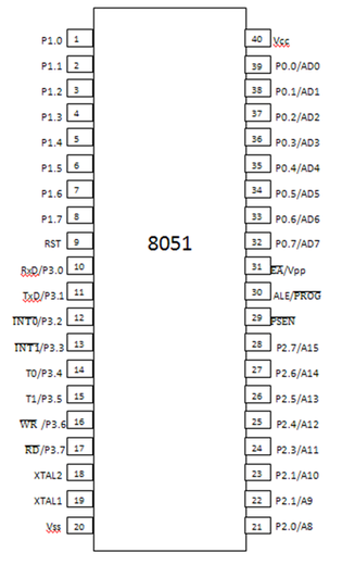
Pin Functions
Reset (Pin 9)
It is an active high input. The circuit diagram is as shown above. It is used for initialization of the 8051 system
It is an active low input.
It is used to allow or disallow the internal memory.
When ‘0’ ------ Internal memory is not used
When ‘1’ ------ Internal memory is used
It is an active low input.
It is used to allow or disallow the external memory.
When ‘0’ ------ external memory is not used
When ‘1’ ------ external memory is used
It is an active high input control signal.
ALE signal is used for demultiplexing the multiplexed Address/Data bus of Port 0 during external memory interfacing.
In each machine cycle, there are 2 ALE pulses
ALE is also used to check whether the device is working or not.
External pull up registers are required to function properly as input or output.
Lower order Address bus (AD0-AD7) is multiplexed during external memory interfacing.
The registers are internally pulled up.
Port 1 does not offer any alternate functions.
The registers are internally pulled up.
Higher order Address bus is multiplexed during external memory interfacing.
Pin 10: RXD Serial asynchronous communication input or Serial synchronous communication output.
Pin 11: TXD Serial asynchronous communication output or Serial synchronous communication clock output.
Pin 12: INT0 Interrupt 0 input.
Pin 13: INT1 Interrupt 1 input.
Pin 14: T0 Counter 0 clock input.
Pin 15: T1 Counter 1 clock input.
Pin 16: WR Write to external (additional) RAM.
Pin 17: RD Read from external RAM.
- XTAL1 & XTAL2 (Pin 18 & 19)
- VCC (Pin 40)
- VSS (Pin 20)
Reset (Pin 9)
It is an active high input. The circuit diagram is as shown above. It is used for initialization of the 8051 system
- EA(bar)
It is an active low input.
It is used to allow or disallow the internal memory.
When ‘0’ ------ Internal memory is not used
When ‘1’ ------ Internal memory is used
- PSEN (bar)
It is an active low input.
It is used to allow or disallow the external memory.
When ‘0’ ------ external memory is not used
When ‘1’ ------ external memory is used
- ALE
It is an active high input control signal.
ALE signal is used for demultiplexing the multiplexed Address/Data bus of Port 0 during external memory interfacing.
In each machine cycle, there are 2 ALE pulses
ALE is also used to check whether the device is working or not.
- Port 0
External pull up registers are required to function properly as input or output.
Lower order Address bus (AD0-AD7) is multiplexed during external memory interfacing.
- Port 1
The registers are internally pulled up.
Port 1 does not offer any alternate functions.
- Port 2
The registers are internally pulled up.
Higher order Address bus is multiplexed during external memory interfacing.
- Port 3
Pin 10: RXD Serial asynchronous communication input or Serial synchronous communication output.
Pin 11: TXD Serial asynchronous communication output or Serial synchronous communication clock output.
Pin 12: INT0 Interrupt 0 input.
Pin 13: INT1 Interrupt 1 input.
Pin 14: T0 Counter 0 clock input.
Pin 15: T1 Counter 1 clock input.
Pin 16: WR Write to external (additional) RAM.
Pin 17: RD Read from external RAM.
