Crystal Structure
Matter exist usually in solid or fluid (liquid, gas) state. According to modern concept matter classification is specified as condensed state and gaseous state. Solids and liquids come under condensed state. Any material whose position of constituent particles is fixed can be regarded as solids.
Solids are characterized by incompressibility, rigidity and mechanical strength. This indicates that the molecules, atoms or ions that make up as solid is closely packed. Thus in solids we will have a well ordered molecular, atomic or ionic arrangement.
In general solids can be classified into:
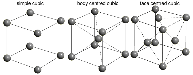
If the atoms or molecules are uniquely arranged in crystalline solid or liquid we call it as a crystal structure. A crystal posses long range order and symmetry. The main property of crystal structure is its periodicity. This periodicity is due to the arrangement of atoms/molecules in the lattice points. The crystal structure as a whole can be considered as the repetition of unit cell. For a given crystal structure the shape of unit cell is same but varies from crystal to crystal.
Lattice
A crystal structure is formed only when the group of atoms is arranged identically at the lattice point. The group of atoms or molecules is called a basis. Lattice point is actually an imaginary concept.
Unit cell
Unit cell can be considered as the building block of a crystal. It has the same symmetry as the entire crystal.
Solids are characterized by incompressibility, rigidity and mechanical strength. This indicates that the molecules, atoms or ions that make up as solid is closely packed. Thus in solids we will have a well ordered molecular, atomic or ionic arrangement.
In general solids can be classified into:
- Crystalline-particles are orderly arranged (long range order).
- Amorphous-particles are randomly oriented.
If the atoms or molecules are uniquely arranged in crystalline solid or liquid we call it as a crystal structure. A crystal posses long range order and symmetry. The main property of crystal structure is its periodicity. This periodicity is due to the arrangement of atoms/molecules in the lattice points. The crystal structure as a whole can be considered as the repetition of unit cell. For a given crystal structure the shape of unit cell is same but varies from crystal to crystal.
Lattice
A crystal structure is formed only when the group of atoms is arranged identically at the lattice point. The group of atoms or molecules is called a basis. Lattice point is actually an imaginary concept.
Unit cell
Unit cell can be considered as the building block of a crystal. It has the same symmetry as the entire crystal.
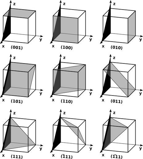
Miller Indices
These are the symbolic vector representations for the orientation of an atomic plane in a crystal lattice and are defined as the reciprocals of the fractional intercepts which the plane makes with the crystallographic axes.
These are the symbolic vector representations for the orientation of an atomic plane in a crystal lattice and are defined as the reciprocals of the fractional intercepts which the plane makes with the crystallographic axes.
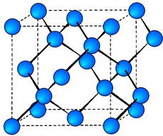
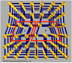
Silicon Crystal Structure
Silicon crystallizes in the same pattern as diamond, two merged FCC cells offset by a/4 in x, y and z.Each atom is individually covalently bonded to four nearest neighbours. The cube side for silicon is 0.543 nm.
14 electrons occupying the 1st 3 energy levels:
–1s, 2s, 2p orbitals filled by 10 electrons
–3s, 3p orbitals filled by 4 electrons
To minimize the overall energy, the 3s and 3p orbitals hybridize to form 4 tetrahedral 3sp orbitals
Each Si atom has 4 nearest neighbors
Lattice constant= 5.431Å
14 electrons occupying the 1st 3 energy levels:
–1s, 2s, 2p orbitals filled by 10 electrons
–3s, 3p orbitals filled by 4 electrons
To minimize the overall energy, the 3s and 3p orbitals hybridize to form 4 tetrahedral 3sp orbitals
Each Si atom has 4 nearest neighbors
Lattice constant= 5.431Å
How Many Silicon Atoms per cm^(-3)?
• Number of atoms in a unit cell:
• 4 atoms completely inside cell
• Each of the 8 atoms on corners are shared among cells - count as 1 atom inside cell
• Each of the 6 atoms on the faces are shared among 2 cells - count as 3 atoms inside cell
Total number inside the cell = 4 + 1 + 3 = 8
• Cell volume: (.543 nm)3 = 1.6 x 10⁻²² cm3
• Density of silicon atoms = (8 atoms) / (cell volume) = 5 x 10²² atoms/cm3
Crystal Orientation
•Two main orientations used in manufacturing integrated circuits are (111) and (100)
•Meaning that the crystal terminates at the wafer surface on (111) and (100) respectively
•As real devices are always built near surfaces, which crystal plane surface terminates on certainly makes difference in electrical and physical properties.
•(111) easier to grow by CZ method . Hence in early days (111) was used extensively by Bipolar now a days it uses (100) as Bipolar also have shrunken in size.
•Surface Density of atoms are highest in 111; minimum in 100; Therefore 111 oxidize faster than 100
•Interface State density –defects at the interface are more in 111 as some of defects relates to dangling bonds
•Hence all CMOS is done 100- low defects at the surface
•Etch rate depends on orientation- since no of atoms are more in 111 and less in 100.
•In case of implantation, orientation doesn’t matter as we have to implant on SiO2
•Oxidation rate higher in 111 than any other orientation
•Mobility depends on orientation; Electron mobility - highest in 111; Hole mobility- highest in 110
crystal defects
1.Point defects
–Anything other than a silicon atom on crystal lattice constitutes a Point defect
–Crucial role in diffusion & ion implantation and very less in oxidation kinetics
2.Line defects (Dislocations)
3.Area defects (Stacking faults)
4.Volume defects
–Anything other than a silicon atom on crystal lattice constitutes a Point defect
–Crucial role in diffusion & ion implantation and very less in oxidation kinetics
2.Line defects (Dislocations)
3.Area defects (Stacking faults)
4.Volume defects
Point defects
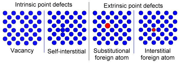
•A point defect in a crystal is an entity that causes an interruption in the lattice periodicity. This occurs during due to following events:
•An atom is removed from its regular lattice site; the defect is a vacancy.
•An atom is in a site different from a regular lattice (substitutional) lattice site; the defect is an interstitial. An interstitial defect can be of the same species as the atoms of the lattice (it is an intrinsic defect, the self-interstitial) or of a different nature ( it is then an extrinsic defect, an interstitial impurity).
•An impurity occupies a substitutional site.
Line defects (Dislocations)
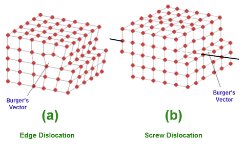
•One-dimensional defects in crystals are known as dislocations. The crystal contains an extra plane of atoms, which terminates at a dislocation. The dislocation itself, then is a linear defect in the direction into the paper. Dislocations either terminate at the edge of the crystal (edge dis- location , or they form a closed loop within the crystal (dislocation loops)
•Dislocations are active defects in crystals, that is they can move when subjected to stresses or when excess point defects are present. The process of "climb" occurs when excess point defects are absorbed by the dislocation
• Sources:
i) by stress due to temperature
gradient
ii) agglomeration
•Dislocations are active defects in crystals, that is they can move when subjected to stresses or when excess point defects are present. The process of "climb" occurs when excess point defects are absorbed by the dislocation
• Sources:
i) by stress due to temperature
gradient
ii) agglomeration
Area defects (Stacking faults)
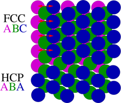
•The most common kind of 2D or area defect found in silicon is the stacking fault.
• Stacking faults always form along {111} planes and are simply the insertion or removal of an extra {111} plane.
•In a perfect crystal, the stacking order is ABCABC, and so on. When a stacking fault is present, either an extra plane is inserted (ABCACBC, etc.) or a plane is missing (ABCABABC)
•Such faults are referred to as "extrinsic" if there is an extra plane of atoms, or "intrinsic" if a plane is missing.
•Stacking faults are bounded by dislocations and, when they intersect the wafer surface, are usually referred to as surface stacking faults.
volume defects
- Three-dimensional macroscopic or bulk defects, such as pores, cracks, or inclusions
- Voids — small regions where there are no atoms, and which can be thought of as clusters of vacancies
