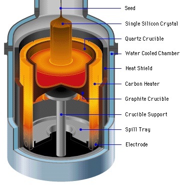
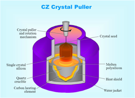
Crystal Growth - Czochralski Method
•First developed by Czochralski (1918)
•Further developed by Teal (early 1950)
•It is solidification of a crystal from a melt
•Quartz (SiO2) is refined electronic grade polysilicon 99.99999% purity
•Fused silica crucible contained in an evacuated chamber is used
•Poly is loaded into crucible
•Chamber is filled with inert gas
•Crucible is heated to approx. 15000C
•Small chemically etched seed crystal is (0.5 cm in diam and 10 cm long) is lowered into contact with the melt
•Larger crystal developed is called boule.
•Modern boules may have 300 mm diam and 1 to 2 m long
•Seed rotates and pulls up the melt to form into crystal
•Crystalline quality is a sensitive function of pull rate
•If pull rate is too low, point defects will increase
•Material near melt has a very high density of point defects. Therefore, solid needs to be cooled quickly to avoid spreading these defects. But rapid cooling means large thermal gradients and leads to high stress
•As the diameter of crystal is increased, the pull rate must be decreased
• Si is purified from SiO2 (sand) by refining, distillation and CVD.
• It contains < 1 ppb impurities. Pulled crystals contain O (~1018 cm-3) and C (~1016 cm-3), plus dopants placed in the melt.
•All Si wafers come from “Czochralski” grown crystals.
•Polysilicon is melted, then held just below 1417 °C, and a single crystal seed starts the growth.
•Pull rate, melt temperature and rotation rate control the growth
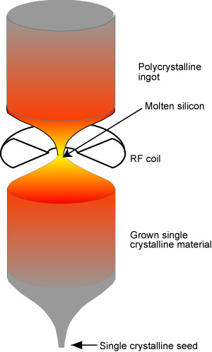
Float Zone
An alternative process is the “Float Zone” process which can be used for refining or single crystal growth.
In the float zone process, dopants and other impurities are rejected by the regrowing silicon crystal. Impurities tend to stay in the liquid and refining can be accomplished, especially with multiple passes.