Phototransistor
A photodiode cannot provide any type of amplification, hence phototransistors are used. A phototransistor can provide the internal current multiplication and generate a larger output signal.
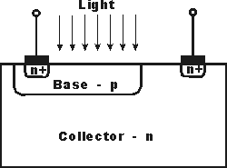
Construction
· Light is allowed to fall on the collector-base junction of the transistor.
· Photocurrent produced acts as the base current and gets multiplied β times.
Ic = β*IB
· Phototransistors are made using type 3 & 4 materials such as GaAs.
· Heterojunctions are also used as they provide better conversion efficiency.
· These devices are generally made using ion implantation and diffusion techniques.
· In order to ensure optimum conversion, the emitter contact is often offset within the phototransistor structure.
· This ensures maximum light reaches the active area of the phototransistor.
Working
· Phototransistors are operated in their active region.
· The base connected is left open circuit or is disconnected because it is not required.
· The biasing conditions are quite simple.
· Collector of npn transistor is used as +ve terminal and collector of pnp transistor is used as -ve terminal.
· Light enters the base region of the phototransistor.
· There it causes generation of electron-hole pairs in the reverse biased collector-base junction.
· The electron-hole pairs move under the influence of electric field and provide base current
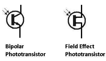
Symbol
Advantages
· Produce higher current than photodiodes
· Phototransistors have a faster operation
· Less cost
· They have a high gain in output
Disadvantages
· Phototransistors made up of Si cannot handle voltages about 1000V
· They do not allow electrons to move freely as in electron tubes
· Thy are vulnerable to electrical spikes and electromagnetic energy
Applications
· Smoke detectors
· Infrared receivers
· CD players
· Astronomy and night vision
· Laser range finding

|

|
