Electronic Devices & Circuits
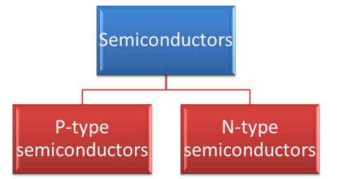
Semiconductors
· A semiconductor material has an electrical conductivity value between a conductor, such as copper, and an insulator, such as glass.
· Semiconductors are the foundation of modern electronics.
· The modern understanding of the properties of a semiconductor relies on quantum physics to explain the movement of electrons and holes in a crystal lattice.
· The electrical conductivity of a semiconductor material increases with increasing temperature, which is behaviour opposite to that of a metal.
· Semiconductor devices can display a range of useful properties such as passing current more easily in one direction than the other, showing variable resistance, and sensitivity to light or heat.
Types of semiconductors
P type semiconductor
In p-type semiconductors, holes are the majority carriers and electrons are the minority carriers. P-type semiconductors are created by doping an intrinsic semiconductor with acceptor impurities.
N type semiconductor
In n-type semiconductors, electrons are the majority carriers and holes are the minority carriers. N-type semiconductors are created by doping an intrinsic semiconductor with donor impurities.
Formation of a P-N junction
· When the N-type semiconductor and P-type semiconductor materials are first joined together a very large density gradient exists between both sides of the PN junction.
· The result is that some of the free electrons from the donor impurity atoms begin to migrate across this newly formed junction to fill up the holes in the P-type material producing negative ions.
· However, because the electrons have moved across the PN junction from the N-type silicon to the P-type silicon, they leave behind positively charged donor ions ( ND ) on the negative side and now the holes from the acceptor impurity migrate across the junction in the opposite direction into the region where there are large numbers of free electrons.
· As a result, the charge density of the P-type along the junction is filled with negatively charged acceptor ions ( NA ), and the charge density of the N-type along the junction becomes positive. This charge transfer of electrons and holes across the PN junction is known as diffusion.
· This process continues back and forth until the number of electrons which have crossed the junction have a large enough electrical charge to repel or prevent any more charge carriers from crossing over the junction.
· Eventually a state of equilibrium (electrically neutral situation) will occur producing a “potential barrier” zone around the area of the junction as the donor atoms repel the holes and the acceptor atoms repel the electrons.
· Since no free charge carriers can rest in a position where there is a potential barrier, the regions on either sides of the junction no become completely depleted of any more free carriers in comparison to the N and P type materials further away from the junction. This area around the PN Junction is now called the Depletion Layer.
Depletion Region
When a p-n junction is formed, some of the free electrons in the n-region diffuse across the junction and combine with holes to form negative ions. In so doing they leave behind positive ions at the donor impurity sites.
· In the p-type region there are holes from the acceptor impurities and in the n-type region there are extra electrons.
· When a p-n junction is formed, some of the electrons from the n-region which have reached the conduction band are free to diffuse across the junction and combine with holes.
· Filling a hole makes a negative ion and leaves behind a positive ion on the n-side. A space charge builds up, creating a depletion region which inhibits any further electron transfer unless it is helped by putting a forward bias on the junction.
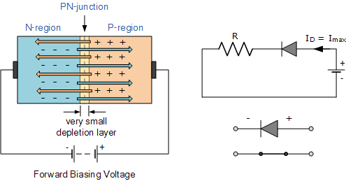
Forward biased P-N junction diode
· Forward bias refers to the application of voltage across the device such that the electric field at the junction is reduced.
· By applying a positive voltage to the p-type material and a negative voltage to the n-type material, an electric field with opposite direction to that in the depletion region is generated.
· Since the resistivity of the depletion region is much higher than that in the remainder of the device, nearly all of the applied electric field is dropped across the depletion region.
· The net electric field is the difference between the existing field in the depletion region and the applied field, thus reducing the net electric field in the depletion region.
· Reducing the electric field disturbs the equilibrium existing at the junction, reducing the barrier to the diffusion of carriers from one side of the junction to the other and increasing the diffusion current.
· While the diffusion current increases, the drift current remains essentially unchanged since it depends on the number of carriers generated within a diffusion length of the depletion region or in the depletion region itself.
· Since the depletion region is only reduced in width by a minor amount, the number of minority carriers swept across the junction is essentially unchanged.
Reverse biased P-N junction diode
· In reverse bias a voltage is applied across the device such that the electric field at the junction increases.
· The higher electric field in the depletion region decreases the probability that carriers can diffuse from one side of the junction to the other, hence the diffusion current decreases.
· As in forward bias, the drift current is limited by the number of minority carriers on either side of the p-n junction and is relatively unchanged by the increased electric field.
· A small increase in the drift current is experienced due to the small increase in the width of the depletion region.
· A semiconductor material has an electrical conductivity value between a conductor, such as copper, and an insulator, such as glass.
· Semiconductors are the foundation of modern electronics.
· The modern understanding of the properties of a semiconductor relies on quantum physics to explain the movement of electrons and holes in a crystal lattice.
· The electrical conductivity of a semiconductor material increases with increasing temperature, which is behaviour opposite to that of a metal.
· Semiconductor devices can display a range of useful properties such as passing current more easily in one direction than the other, showing variable resistance, and sensitivity to light or heat.
Types of semiconductors
P type semiconductor
In p-type semiconductors, holes are the majority carriers and electrons are the minority carriers. P-type semiconductors are created by doping an intrinsic semiconductor with acceptor impurities.
N type semiconductor
In n-type semiconductors, electrons are the majority carriers and holes are the minority carriers. N-type semiconductors are created by doping an intrinsic semiconductor with donor impurities.
Formation of a P-N junction
· When the N-type semiconductor and P-type semiconductor materials are first joined together a very large density gradient exists between both sides of the PN junction.
· The result is that some of the free electrons from the donor impurity atoms begin to migrate across this newly formed junction to fill up the holes in the P-type material producing negative ions.
· However, because the electrons have moved across the PN junction from the N-type silicon to the P-type silicon, they leave behind positively charged donor ions ( ND ) on the negative side and now the holes from the acceptor impurity migrate across the junction in the opposite direction into the region where there are large numbers of free electrons.
· As a result, the charge density of the P-type along the junction is filled with negatively charged acceptor ions ( NA ), and the charge density of the N-type along the junction becomes positive. This charge transfer of electrons and holes across the PN junction is known as diffusion.
· This process continues back and forth until the number of electrons which have crossed the junction have a large enough electrical charge to repel or prevent any more charge carriers from crossing over the junction.
· Eventually a state of equilibrium (electrically neutral situation) will occur producing a “potential barrier” zone around the area of the junction as the donor atoms repel the holes and the acceptor atoms repel the electrons.
· Since no free charge carriers can rest in a position where there is a potential barrier, the regions on either sides of the junction no become completely depleted of any more free carriers in comparison to the N and P type materials further away from the junction. This area around the PN Junction is now called the Depletion Layer.
Depletion Region
When a p-n junction is formed, some of the free electrons in the n-region diffuse across the junction and combine with holes to form negative ions. In so doing they leave behind positive ions at the donor impurity sites.
· In the p-type region there are holes from the acceptor impurities and in the n-type region there are extra electrons.
· When a p-n junction is formed, some of the electrons from the n-region which have reached the conduction band are free to diffuse across the junction and combine with holes.
· Filling a hole makes a negative ion and leaves behind a positive ion on the n-side. A space charge builds up, creating a depletion region which inhibits any further electron transfer unless it is helped by putting a forward bias on the junction.
Forward biased P-N junction diode
· Forward bias refers to the application of voltage across the device such that the electric field at the junction is reduced.
· By applying a positive voltage to the p-type material and a negative voltage to the n-type material, an electric field with opposite direction to that in the depletion region is generated.
· Since the resistivity of the depletion region is much higher than that in the remainder of the device, nearly all of the applied electric field is dropped across the depletion region.
· The net electric field is the difference between the existing field in the depletion region and the applied field, thus reducing the net electric field in the depletion region.
· Reducing the electric field disturbs the equilibrium existing at the junction, reducing the barrier to the diffusion of carriers from one side of the junction to the other and increasing the diffusion current.
· While the diffusion current increases, the drift current remains essentially unchanged since it depends on the number of carriers generated within a diffusion length of the depletion region or in the depletion region itself.
· Since the depletion region is only reduced in width by a minor amount, the number of minority carriers swept across the junction is essentially unchanged.
Reverse biased P-N junction diode
· In reverse bias a voltage is applied across the device such that the electric field at the junction increases.
· The higher electric field in the depletion region decreases the probability that carriers can diffuse from one side of the junction to the other, hence the diffusion current decreases.
· As in forward bias, the drift current is limited by the number of minority carriers on either side of the p-n junction and is relatively unchanged by the increased electric field.
· A small increase in the drift current is experienced due to the small increase in the width of the depletion region.
